Articles

Electronics, mechanical design, and experiments.

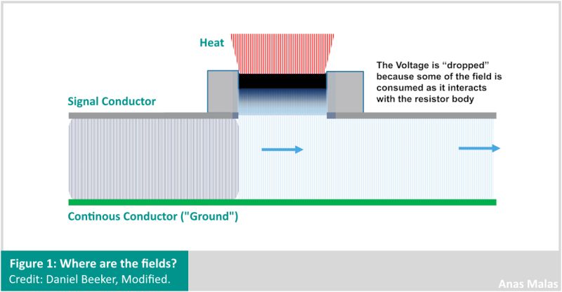
PCB signal field interacting with a resistor body and continuous ground conductor

The resistors on my PCB perplexed me. They demanded "better access to the fields" and "a cleaner environment", how could I resist?

The resistors on my PCB perplexed me. They demanded "better access to the fields" and "a cleaner environment", how could I resist?

During PCB West 2024, two talks gave me reasons to remove copper, soldermask, and silkscreen from under my 2-pin components (resistors, capacitors, etc) for different reasons I hadn't considered. Let's explore why.

Preface: Today, PCB design cannot be treated like laying wires. Almost all modern PCBs contain signals with high frequency content. For those, it is important to have a nearby uninterrupted "return" where "return current" will flow. The closer the two are together, the lower inductance will be.

But where is the energy really contained? Is it the current in your traces? Is it in the voltage?

Daniel Beeker made his intention to brainwash us clear, repeating "Its all about the space". His daughter even made a song about it https://lnkd.in/dTfCfd23

The energy in any electric circuit is contained within the EM field in the dielectric (the insulator). In your PCB that's the fiberglass-resin between your copper layers, and in a grid transmission line that is air. So if the field is between a trace on layer 1 and a ground plane on layer 2, what happens when it reaches a resistor?

As the fields of your signal propagate, they reach the resistor and use use its body as a continuation of the trace, as seen in figure 1. If there is a ground flood on layer 1 and it goes under a resistor, this impedes the field (especially for signals with high frequency content). Capacitors store and release fields which should be able to go in and out with the least impedance, which you can achieve by using the smallest possible capacitor package and exposing its body to the adjacent plane.

Worse yet, running traces under resistors causes crosstalk. This may be fine for slow analog signals, but digital signals are very fast. Adding a keepout in your footprints prevents copper under your components and solves this issue (do however add a copper island with ground vias under ICs).

In another session, Caleb Buck shared his experience in design for reliability, with a focus on flux types and residues. Caleb did a series of tests using methods like "SIR" to test footprints for residue retention. While no-clean flux residue has the lowest (but present) chance of failure, cleaning most components with water or chemicals was sufficient to remove the residues. However, some components did retain flux after cleaning, especially resistors and capacitors. This is because the body of these components rests directly on the PCB with no gap, as seen in figure 2.

The solution is simple. By removing copper, silkscreen, and soldermask from under and a resistor's body, there is enough room for cleaning these residues. QFN packages have a similar issue, and using diagonal silkscreen lines can help lift the package slightly and channel cleaning fluid in.

Small, simple changes, towards designs that work right the first time.
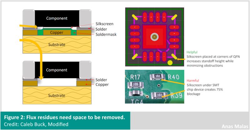
Component cross sections and QFN examples showing clearance for cleaning flux residues
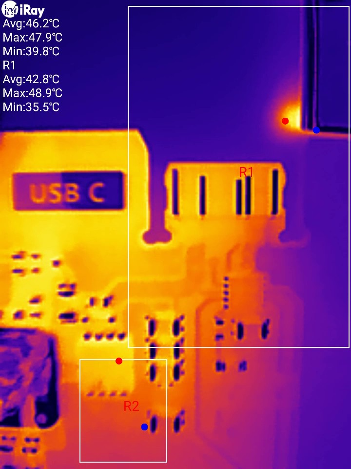
Thermal test of the PCB edge USB-C connector

Compromises and trade offs are an important part of design, but how can you make a good choice without the data to back it?

Compromises and trade offs are an important part of design, but how can you make a good choice without the data to back it?

The data is now here! 100+ mating cycles later, I have included microscope photos, thermal tests, and measured how much force it takes to break this connector. All updates are on GitHub: https://lnkd.in/djgccZi8 My previous post talked about why I created these footprints (https://lnkd.in/dJ2t59Rx). I am very grateful for the large engagement on here and on X!

Hackaday even wrote an article about it, and it was within the top page on Hacker news! I love that this could potentially be helpful to so many, but as many in the replies pointed out: This is a much less durable connector, and you should keep that in mind before deciding to use it! While I had tested the connector on my contact card, I did not document it at the time.

You can find the new tests and a new 24 pin fully featured KiCad footprint in the GitHub repo linked above, and please tag me when you post about the cool stuff you make with this :)

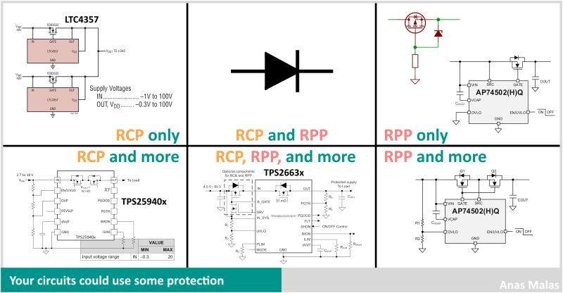
Comparison chart of integrated circuits that provide reverse-voltage, reverse-current, and related circuit protections

Let's go on a journey and look at different types of circuit protection!

Let's go on a journey and look at different types of circuit protection!

“Welcome, Electron! I didn’t expect you coming this way. This is the positive input to the circuit… Tell you what, youre here now, so please have a seat in our little waiting lounge. We don’t normally let electrons this way, but we might be able to work some leakage out”

That’s the story of Edison, who goes by Ed, an electron that’s now stuck at the parasitic capacitance of an input protection circuit. In an ideal world, the user wouldn’t have reversed the voltage to the circuit and sent Ed the wrong way. But things go wrong all the time, and while Ed and his friends mean well, they could do a lot of damage if allowed to go through.

Circuit protection is a field that looked easy enough to me from the outside, but I found that there are subtle differences in capabilities that can make or break it, depending on your circuit's needs. So, what might your circuit need?

- You might need Reverse Current Protection (RCP). A charger port shouldn’t be live, and a series diode could solve this if you can tolerate the voltage drop and power dissipation. When you need more current or less voltage drop, you can use an ideal diode controller chip, a type of Power Management IC (PMIC).

- You might need Reverse Polarity Protection (RPP). A high side PMOS circuit works, though you might need to use an NMOS for better performance. In that case, you could use a high side NMOS with a PMIC that provides RPP by using a charge pump. A low side NMOS could do the job, but cutting ground is risky.

- Some applications need both, others require one but not the other. If your user can access the battery connector, you might want RPP without RCP to enable battery charging. Some RCP circuits cannot handle reverse polarity themselves.

A PMIC can provide more than just RPP and RCP. Here are some useful features that you might also want, or which you might want to avoid if they would interfere with the intended circuit function:

- Load power switching

- Over current protection (OCP)

- Shortcircuit protection (which may not be covered adequately by OCP)

- Soft start (for high circuit capacitance or when slew rate control is needed)

- Overvoltage protection (OVP), as either a lockout that disconnects the output or a surge clamp that attempts to keep the lights on

- Undervoltage lockout (UVLO)

- Automotive load dump protection

It’s important to not just take the specs at face value, always evaluate how the protection works and acts, especially in context of your circuit. For example, downstream inductance may necessitate a reverse clamp diode on the PMIC output. Leakage is another thing to watch out for, on just 60 uA of Schottky leakage, I had a high efficiency LED light up brightly! It’s a funny problem to have from such a small amount of Ed’s friends, but it could be worse!

All writing and information is mine, no AI here. let me know if I missed anything!

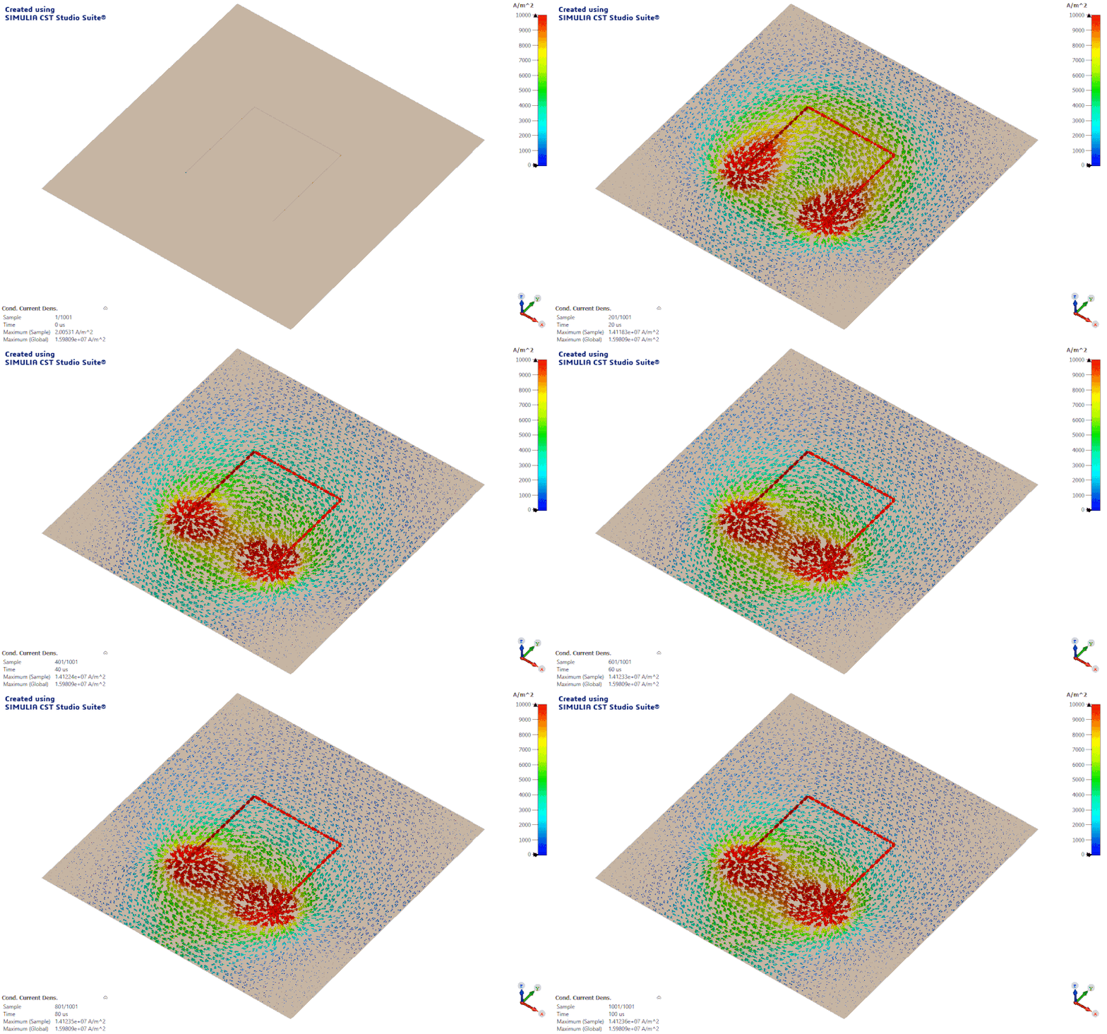
PCB cross section illustrating a high-frequency return current path

To design a good PCB, you've got to understand this!

To design a good PCB, you've got to understand this!

Return current is the current flowing back to complete the circuit. If it is on a copper plane, it gets concentrated on the path of least impedance. The amazing thing is that it is frequency dependent, so when the current changes in a short amount of time (high edge frequency), its return current on the return plane runs exactly under the signal as that's the least impedance path (lowest industance and highest capacitance).

Some time after the sudden current step, the signal current is still flowing steadily, at that point we start to go towards a DC condition in which the path of least impedance is just the path of least ohmic resistance, which happens to be a wide copper area directly between the two points.

What an amazing visualization.

Circuit board cross section with return-current guidance

Remember when you didn't need to care about return currents? I don't, I was born after!

Remember when you didn't need to care about return currents? I don't, I was born after!

Integrated circuits (ICs) keep getting smaller and faster, so it is increasingly important to design circuit boards correctly.

Firstly, if you dont understand return currents well, I implore you to watch the presentation that changed my life, by Rick Hartley: https://lnkd.in/dECCj99s

I have talked to many designers who know return currents, but recommend counter-productive stackups. Let's start with a basic fact: A signal layer must have an adjacent, relevant, and close return plane. When you move a signal through layers, so does the return. how it does so is the question.

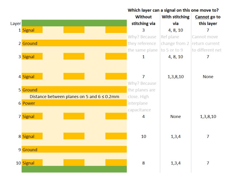
The first attached stackup photo is a 10 layer stackup taken from Susy Webb's presentation: https://lnkd.in/dP8Wph5C. It illustrates the cases you could face in any design. A signal on layer 1 has its return on layer 2, with the energy traveling in the dielectric between them. If you move the signal to layer 3, the energy will pass through the barrel's antipad and continue between layers 2 and 3. The current doesnt change layers, and the energy doesnt spread.

On the other hand, say you want to move a signal from layer 1 to 8. If you dont include a stitching via that connects the grounds on layers 2 and 9, the return current will spread wide and "force" itself through your circuit until it finds layer 9. A stitching via provides a good path and the energy wont spread.

But you'll see something interesting, how can a signal on layer 4 go to 7 at all? The distance between the two planes is small, so the return current can find enough capacitance to flow without spreading widely (remember, C∝A). However, going from layer 7 to 8 doesnt work well, as you cannot directly stitch or couple layers 6 and 9 together.

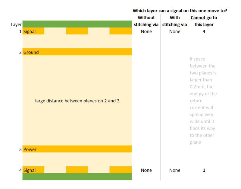
That brings us to the first 4 layer stackup. See the issue? The planes are far away so if the signal changes layers from 1 to 4, the return current will spread very far until it finds enough capacitance to couple from layer 2 to 3. Some designers recommend this with "layer change capacitors" to move the return from layer 2 to 3.

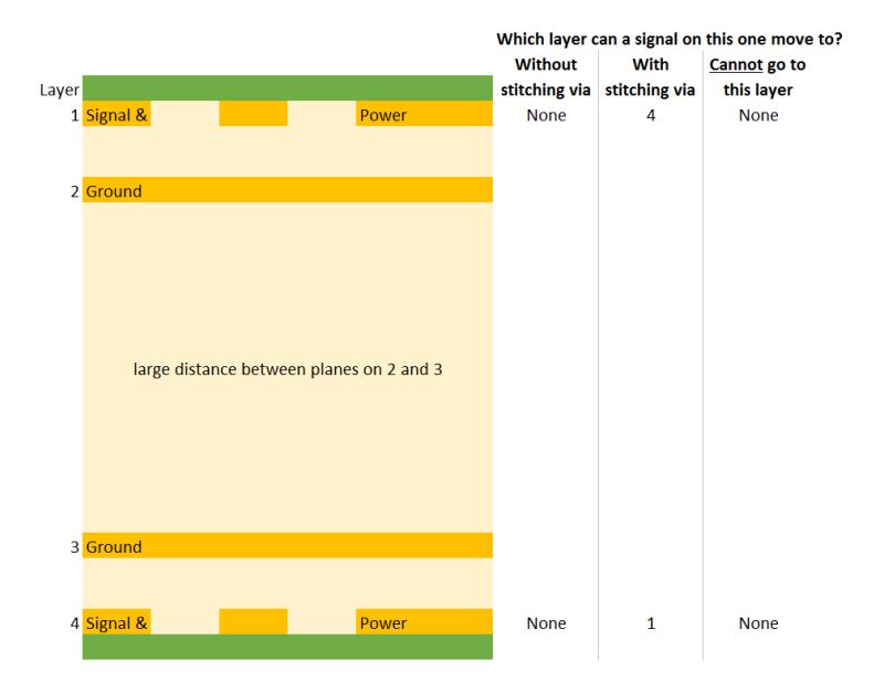
However, looking at a $0.5 mcu's (Attiny5) IBIS model reveals that its rising waveform can be as fast as 1 ns (no load). That's an edge frequency of 1 GHz, and a 0402 0.1 uF capacitor resonates below 30 MHz, not to mention via inductance. The second 4 layer stackup allows for stitching vias and provides a return to power, which is why I believe it is better for today's designs.

Here's where id appreciate some help. In an article, Lee Ritchey said that stitching vias aren't necessary. I believe he's talking about high density designs which have tons of ground vias anyway, but that's speculation. Also, in the 10L stackup even if layer 3 is twice nearer to its reference than layer 4, wouldnt there be crosstalk between them?

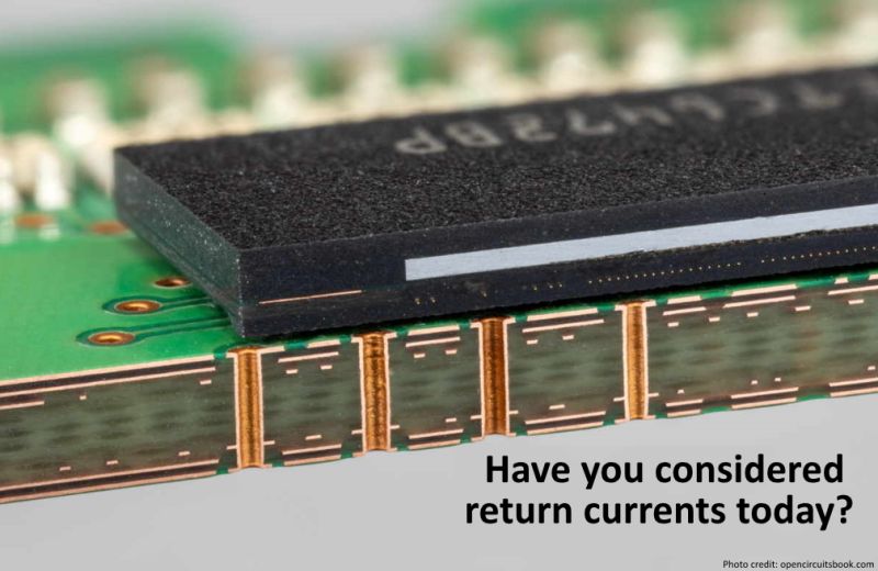
Cover photo taken from opencircuitsbook.com. Excited to get my copy!

10 layer good stackup
Bad 4 layer stackup
Good 4 layer stackup
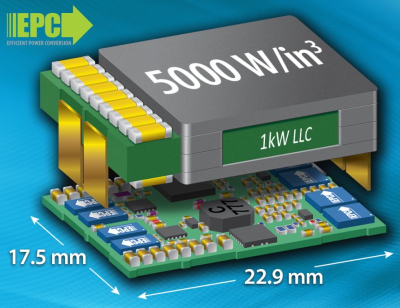
A small 1 kW GaN power converter shown beside its power-density claim

Silicon must watch out, GaN's in town and it's coming for the crown!

Silicon must watch out, GaN's in town and it's coming for the crown!

Well... The performance and miniaturization in power electronics crown, but who's counting. Last year as part of my bachelors I had to write a review paper. There was a big marketing boom in tiny USB-C "chargers" attributing their size to GaN (Gallium Nitride), which I wanted to investigate. Now, I think that in 5-10 years, all of our devices will have a GaN powerstage.

But first, what even is it? The MOSFET we all know and love is built with silicon using P/N junctions. GaN is also a semiconductor, but it has a wide-bandgap which allows operation at higher voltages and smaller devices. Not only that, but an AlGaN layer induces a highly conductive layer of electrons (called 2DEG) which reduces resistance. But the star feature of GaN is the low switching losses, allowing cool operation at very high frequencies.

All in all, this means that GaN transistors can be made relatively tiny with very low Rds(on), high current carrying capacity, and low parasitic capacitance. But there are mature Silicon parts with even lower Rds(on) than the current young GaN market, so why go with GaN? In a Silicon MOSFET, low Rds(on) necessitates a large gate and thus high parasitic capacitance, resulting in high switching losses at high frequencies.

But why would I want a high switching frequency? A power converter relies on storage elements: capacitors and inductors. A high switching frequency means that each cycle is shorter, thus less energy needs to be stored. Less energy means smaller L and C, thus smaller passives. 1+kW GaN power converters are demonstrated in credit card sizes with MLCC only capacitors!

Here's the exciting part. During my search, I found many examples for power converters with GaN transistors being much smaller. For example, I compared two AC/DC forced air cooled power converters. The 4kW GaN model was 1.9x heavier and 1.1x bigger than a 1kW super-junction silicon model. More exciting is this module under development at EPC - Efficient Power Conversion (GaN transistor company) that has a 1 kW capacity with a footprint SMALLER than 1x1"!

One distinction to make is that GaN transistors aren't MOSFETs. Most GaN structures don't use P/N junctions. The nearest device to a Si MOSFET is a GaN HEMT (High-electron-mobility transistor) but it is normally-on and isnt doped. There are many structures that solve the normally-on issue such as cascode, GIT, finFET, pillar, and other commercial and research grade transistors.

So, will GaN replace Si? No. GaN is more expensive to fabricate (especially vertically, without a different substrate like Si or SiC). It is unlikely to be cheaper for applications that dont benefit from a faster switching or a small footprint. I believe that most future power converters will be GaN based, but silicon will still dominate the power marketshare. Have you used GaN? How has your experience been?

Presentation image about pink ESD protective bags

Sometimes old is gold, but it's 𝘴𝘩𝘰𝘤𝘬𝘪𝘯𝘨𝘭𝘺 quite pink in this presentation.

Sometimes old is gold, but it's 𝘴𝘩𝘰𝘤𝘬𝘪𝘯𝘨𝘭𝘺 quite pink in this presentation.

Speaking of shocks, if you work in electronics, you probably know what Electrostatic Discharge (ESD) is. I thought I understood it, but this highly entertaining presentation (recorded 20 years before I was born) made me realize that I didnt know ESD all that well.

ESD control came from the (almost literal) aftermath of an unfortunate explosion at Nasa, but as time progressed they realized that electronics also need static control. After looking at microscopic pictures of the silicon dies of failed chips, it was found out that ESD zaps a hole in the dielectric, vaporizes the contact, coats the hole that it just created shorting both contacts together, and killing the chip or part of.

But then you know it is dead, and where's the fun in that? In some cases, the ESD is just the right strength to not cause an immediate short circuit, but it gets very very close. The chip passes QC, is sent out, and dies promptly while in the middle of service. Mishandling of ESD sensitive devices might not even be apparent at first. Sometimes instead of the chip not working correctly, it would work in an unexpected way making troubleshooting harder.

So, why is old pink? because ultimately, pink polyethylene bags were invented by this person. It contains a surfactant which both holds just enough water to not allow the bag to create any static of its own, and self replenishes itself over time to stay effective. The bags were actually clear, but they wanted to dye them red to differentiate them, but instead, we got the pink bags that are commonly used today. However, while these bags dont create static, they cannot protect from external ESD. For that, the metallic bags are used.

These metallic bags can protect from external charges, but they also allow charge to build up when components rub the inside surface. Thus one of the best ways to really protect components is to place them in a pink poly bag while in an ESD safe environment, and then to place that bag inside of a metallic bag.

I suggest that you watch the lecture here, very unique presentation style:

Differential-pair routing examples on a PCB

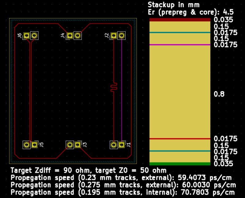
Picture this: you ask an electronics engineer to add 3 differential pairs onto a PCB, and they deliver the following, what do you do?

Picture this: you ask an electronics engineer to add 3 differential pairs onto a PCB, and they deliver the following, what do you do?

If you listen to application notes, you are furious! only one of these is routed how a differential pair should be, right? Well... According to Rick Hartley's presentation titled "What your Differential Pairs Wish You Knew", all three are equally as good! How can this be?!

I cannot explain the full topic as beautifully as Rick did in the hour long presentation and I implore you to watch it (https://lnkd.in/dF4rha6Y), but here is a summary:

On a PCB, differential pairs can be treated as two single ended signals, with most of their coupling being to the ground plane (drawn but unfilled on layer 2). As they are not twisted, having them in close proximity cannot meaningfully cancel out interference, so that is unnecessary. As long as you achieve the target impedance, there is another thing that you should care about: time.

A differential signal has two opposite signals, so it stands to reason that both will transition at the sender at the same time and cross close to the middle of the transition. What matters is that at the receiver, they must cross within 60% of the signal's limits (for example, for a 0-3.3V signal, they must cross between 0.7 and 2.6V), or the signal may fail to be read correctly. Routing the differential lines together is then just a way to get the length close enough that timing is close enough to fall within the 60%, and this is where skew tolerance comes from.

But that is for a perfect PCB, made with a uniform dielectric, which does not exist. FR4 is a weave, and some particular types have spaces in the fiberglass that may mean that two lines may experience very different dielectric constants, which affects the propagation delay and thus when one of the two signals will reach. Stackup selection is thus very important especially when it comes to what dielectric is chosen.

Another factor is inner vs outer layer, as propagation is faster in outer layers, length matching an inner trace with an outer trace does not work, which is why you see that I have added a delay when the other trace was ran on layer 3. The trace on L3 needed to be thinner to have a 90 ohm differential impedance, despite being equidistant to the plane on layer 2 (this is why I choose a 6 layer stackup).

But wait, how can a single trace have a differential impedance? Well, it doesnt. Zdiff = 2*Zodd, and Zodd = Z0 - Zcoupling. When a differential pair is routed together, coupling exists and must be taken into consideration, but when routing the differential pair with uncoupled traces, Zodd = Z0.

So should you stop routing differential pairs together? No. But understanding how a differential pair actually works is important, and if a differential pair needs to not be routed together, so be it.

Thanks Rick for the valuable presentations, and thanks Waseem Alkhayer for pointing out this presentation.

Close comparison of individual resistors and a four-resistor array

Can the cheapest component on a circuit board be made cheaper?

Can the cheapest component on a circuit board be made cheaper?

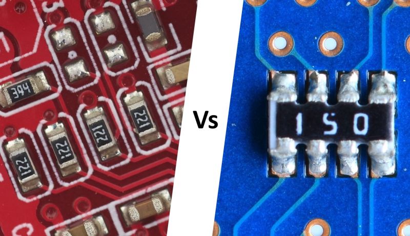
Last week I posted a photo of computer RAM, in which a special component caught my attention. On the blue PCB (printed circuit board), you can see a resistor array containing four resistors of the same value (15 ohm). This is less common than single resistors, such as the four seen on the red board (marked 221, which means 220 ohm). But why choose either one?

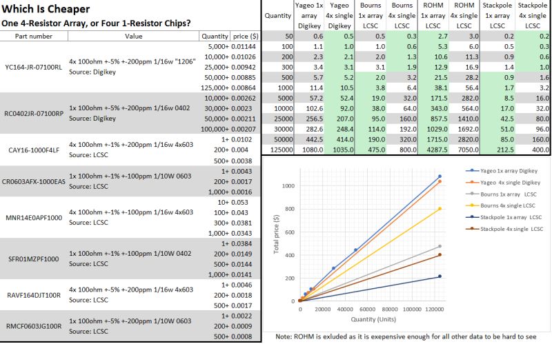
I had previously heard from an experienced engineer that a resistor array can be cheaper, but I wanted to check this claim. I used digikey (American) and LCSC (Chineese) websites to compare, first finding an array, then comparing it to buying four of the closest compareable single resistor. The result of this can be seen in photo 2, in which we can see that in come cases, especially at a higher order amount, the array is indeed cheaper. If a board needs 100 resistors of the same value, and a million units are made over its lifetime, $37,500 can be saved (using 25 stackpole arrays instead of 100 stackpole resistors).

One more reason resistor arrays can be cheaper is the fact that they only require one placement in the pick and palce machine, in low production runs this doesnt mean much, but if the machine is working 24/7 on one single design, it can quickly add up.

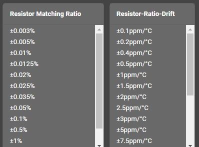
When I posted last week, I was expecting cost to be the primary driver for using arrays, but Eng. Eyas Alsuhaibani pointed out that having the resistors be in an array means that they are better matched. Indeed, as seen in the last photo, arrays can be purchased with specific matching tolerances. Why does this matter? Because even a 0.1% resistor can mean that there is a 0.2% difference, and if the difference between the parts is more important than the absolute resistance, then an array is the better choice.

One reason not to use resistor arrays is that some parameters may not be avaiable, such as low temperature coeffeiceint (200 ppm seems to be the most common, with some 100 ppm parts available, with only one vendor supplying 0.1-1 ppm). This should not matter in most cases, but calculation is necessary to ensure proper device operation.

I have seen many parts such as diodes, mosfets, LEDs, etc in which multiple ones are packaged together, but this seems much less prevalent in capacitors (a capacitor array could be used for things like PCIe, where every device needs DC blocking capacitors). I think it may have to do with crosstalk, what do you think the reason may be?

Price comparison of four-resistor arrays and individual resistor chips
Comparison of resistor matching ratio and resistor-ratio drift
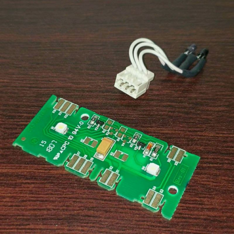
Infrared LED and receiver used to detect whether the mini-fridge door is closed

Recently, my hotel room's mini fridge had a flickering light and a glass door. So instead of going to sleep, I discovered something awesome 📟

Recently, my hotel room's mini fridge had a flickering light and a glass door. So instead of going to sleep, I discovered something awesome 📟

I couldve called reception, but where's the fun in that? Instead I took apart the light assembly to try to see what the issue is, and this is what I found.

As an electronics engineer, and especially as someone who likes working on mass manufactured consumer goods, every little bit of money saved per unit saves the company millions. and here, with ONE connector, a ton of money was saved!

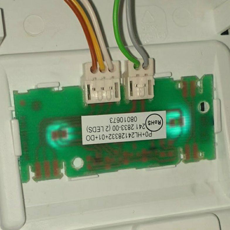
In the photos you can see a connector that was new to me. It belongs to a family called "RAST 2.5", and is made specifically to be as standard and cheap as possible while still being reliable enough even for automotive applications. It replaces the plastic half that is supposed to be on the printed circuit board (PCB)... with the PCB itself! Saving not only the component cost, but also the process cost of soldering it.

But wait, it gets better! If you grab any usual cable that connects to a pcb or those you find in cars, you'll find a plastic plug. This isnt one part, instead, the wires are each stripped, placed inside the metal pins (called terminals), crimped, and then individually inserted into the plastic housing to form the plug (two unique part numbers per plug, excluding the receptical that the plug goes into).

That's where the designers of this connector found yet another opportunity. Instead of the 3 part plug/terminal/receptical you normally find, here there is no terminal for the wires to go into first. The UNstripped wires are placed into the connector, a plunger is pressed in, and the connector itself cuts the plastic insulation and contacts the wires (this connection method is called IDC). This one part is cheaper than buying the normal 3, and installing it is a faster and cheaper process.

In the first photo you can see the IR LED/Reciever that are used to detect the door being closed, in the next, you can see how the single layer board is held in the plastic without screws (saving even more cost) and with two of those connectors on it, and in the last, here's how cheap these connectors are when you buy "just" a thousand. Now imagine buying a million.

Turns out that even a vacation can be educational, and the light stopped blinking after I took it apart and put it back together. So Novotel Hotels, sorry and you're welcome, I guess 😅

Single-layer mini-fridge light PCB held in its plastic enclosure without screws
Distributor pricing shown for the RAST 2.5 insulation-displacement connector