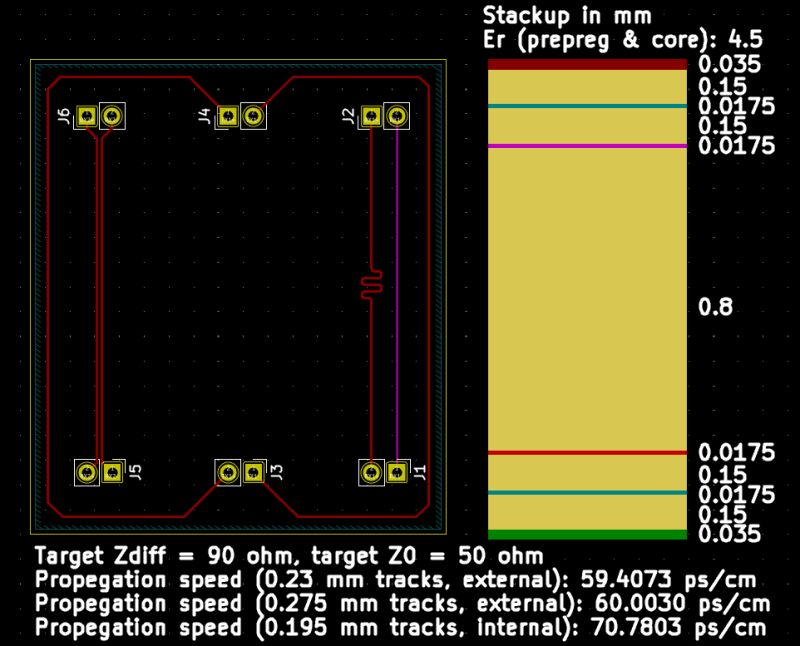
If you listen to application notes, you are furious! only one of these is routed how a differential pair should be, right? Well... According to Rick Hartley's presentation titled "What your Differential Pairs Wish You Knew", all three are equally as good! How can this be?!
I cannot explain the full topic as beautifully as Rick did in the hour long presentation and I implore you to watch it (https://lnkd.in/dF4rha6Y), but here is a summary:
On a PCB, differential pairs can be treated as two single ended signals, with most of their coupling being to the ground plane (drawn but unfilled on layer 2). As they are not twisted, having them in close proximity cannot meaningfully cancel out interference, so that is unnecessary. As long as you achieve the target impedance, there is another thing that you should care about: time.
A differential signal has two opposite signals, so it stands to reason that both will transition at the sender at the same time and cross close to the middle of the transition. What matters is that at the receiver, they must cross within 60% of the signal's limits (for example, for a 0-3.3V signal, they must cross between 0.7 and 2.6V), or the signal may fail to be read correctly. Routing the differential lines together is then just a way to get the length close enough that timing is close enough to fall within the 60%, and this is where skew tolerance comes from.
But that is for a perfect PCB, made with a uniform dielectric, which does not exist. FR4 is a weave, and some particular types have spaces in the fiberglass that may mean that two lines may experience very different dielectric constants, which affects the propagation delay and thus when one of the two signals will reach. Stackup selection is thus very important especially when it comes to what dielectric is chosen.
Another factor is inner vs outer layer, as propagation is faster in outer layers, length matching an inner trace with an outer trace does not work, which is why you see that I have added a delay when the other trace was ran on layer 3. The trace on L3 needed to be thinner to have a 90 ohm differential impedance, despite being equidistant to the plane on layer 2 (this is why I choose a 6 layer stackup).
But wait, how can a single trace have a differential impedance? Well, it doesnt. Zdiff = 2*Zodd, and Zodd = Z0 - Zcoupling. When a differential pair is routed together, coupling exists and must be taken into consideration, but when routing the differential pair with uncoupled traces, Zodd = Z0.
So should you stop routing differential pairs together? No. But understanding how a differential pair actually works is important, and if a differential pair needs to not be routed together, so be it.
Thanks Rick for the valuable presentations, and thanks Waseem Alkhayer for pointing out this presentation.