Well... The performance and miniaturization in power electronics crown, but who's counting. Last year as part of my bachelors I had to write a review paper. There was a big marketing boom in tiny USB-C "chargers" attributing their size to GaN (Gallium Nitride), which I wanted to investigate. Now, I think that in 5-10 years, all of our devices will have a GaN powerstage.
But first, what even is it? The MOSFET we all know and love is built with silicon using P/N junctions. GaN is also a semiconductor, but it has a wide-bandgap which allows operation at higher voltages and smaller devices. Not only that, but an AlGaN layer induces a highly conductive layer of electrons (called 2DEG) which reduces resistance. But the star feature of GaN is the low switching losses, allowing cool operation at very high frequencies.
All in all, this means that GaN transistors can be made relatively tiny with very low Rds(on), high current carrying capacity, and low parasitic capacitance. But there are mature Silicon parts with even lower Rds(on) than the current young GaN market, so why go with GaN? In a Silicon MOSFET, low Rds(on) necessitates a large gate and thus high parasitic capacitance, resulting in high switching losses at high frequencies.
But why would I want a high switching frequency? A power converter relies on storage elements: capacitors and inductors. A high switching frequency means that each cycle is shorter, thus less energy needs to be stored. Less energy means smaller L and C, thus smaller passives. 1+kW GaN power converters are demonstrated in credit card sizes with MLCC only capacitors!
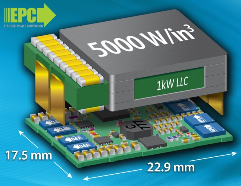
Here's the exciting part. During my search, I found many examples for power converters with GaN transistors being much smaller. For example, I compared two AC/DC forced air cooled power converters. The 4kW GaN model was 1.9x heavier and 1.1x bigger than a 1kW super-junction silicon model. More exciting is this module under development at EPC - Efficient Power Conversion (GaN transistor company) that has a 1 kW capacity with a footprint SMALLER than 1x1"!
One distinction to make is that GaN transistors aren't MOSFETs. Most GaN structures don't use P/N junctions. The nearest device to a Si MOSFET is a GaN HEMT (High-electron-mobility transistor) but it is normally-on and isnt doped. There are many structures that solve the normally-on issue such as cascode, GIT, finFET, pillar, and other commercial and research grade transistors.
So, will GaN replace Si? No. GaN is more expensive to fabricate (especially vertically, without a different substrate like Si or SiC). It is unlikely to be cheaper for applications that dont benefit from a faster switching or a small footprint. I believe that most future power converters will be GaN based, but silicon will still dominate the power marketshare. Have you used GaN? How has your experience been?