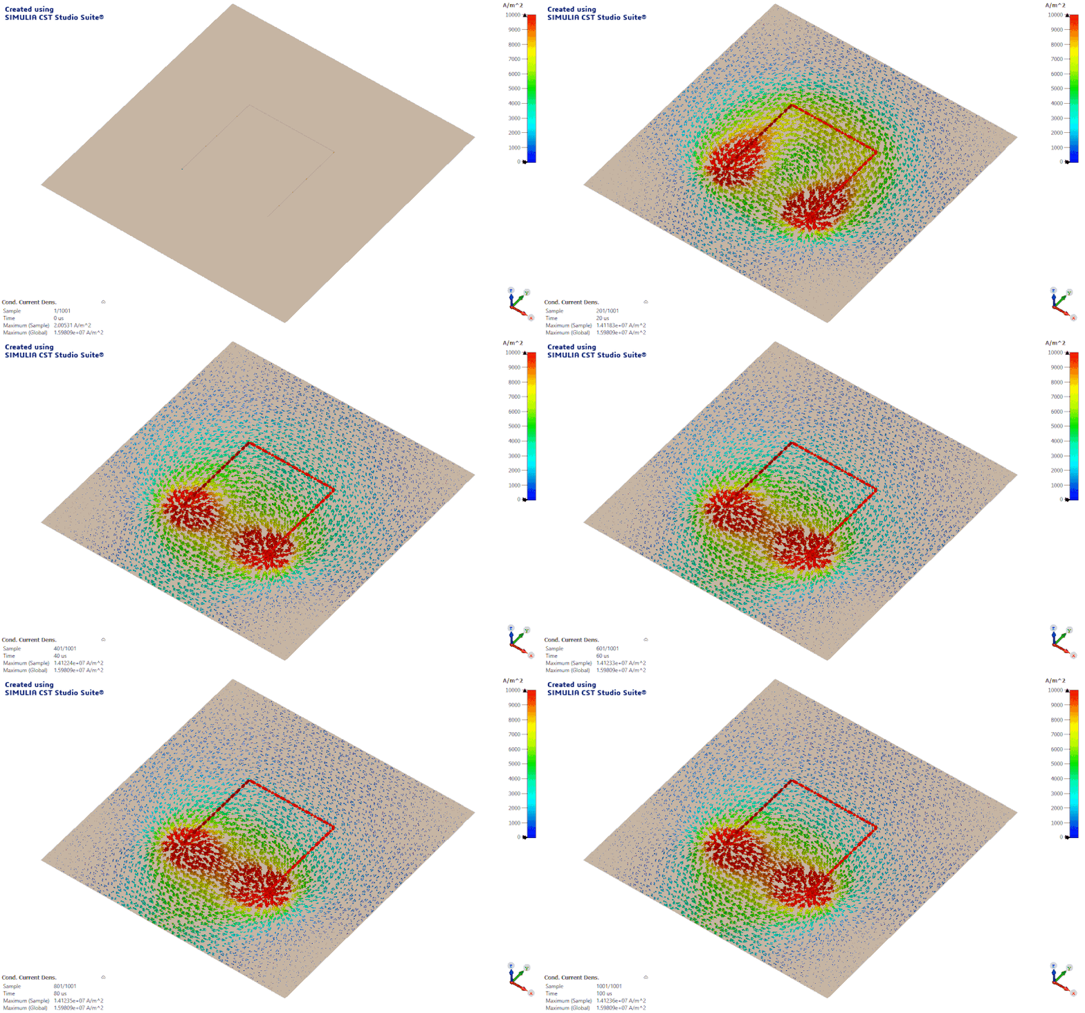
Return current is the current flowing back to complete the circuit. If it is on a copper plane, it gets concentrated on the path of least impedance. The amazing thing is that it is frequency dependent, so when the current changes in a short amount of time (high edge frequency), its return current on the return plane runs exactly under the signal as that's the least impedance path (lowest industance and highest capacitance).
Some time after the sudden current step, the signal current is still flowing steadily, at that point we start to go towards a DC condition in which the path of least impedance is just the path of least ohmic resistance, which happens to be a wide copper area directly between the two points.
What an amazing visualization.