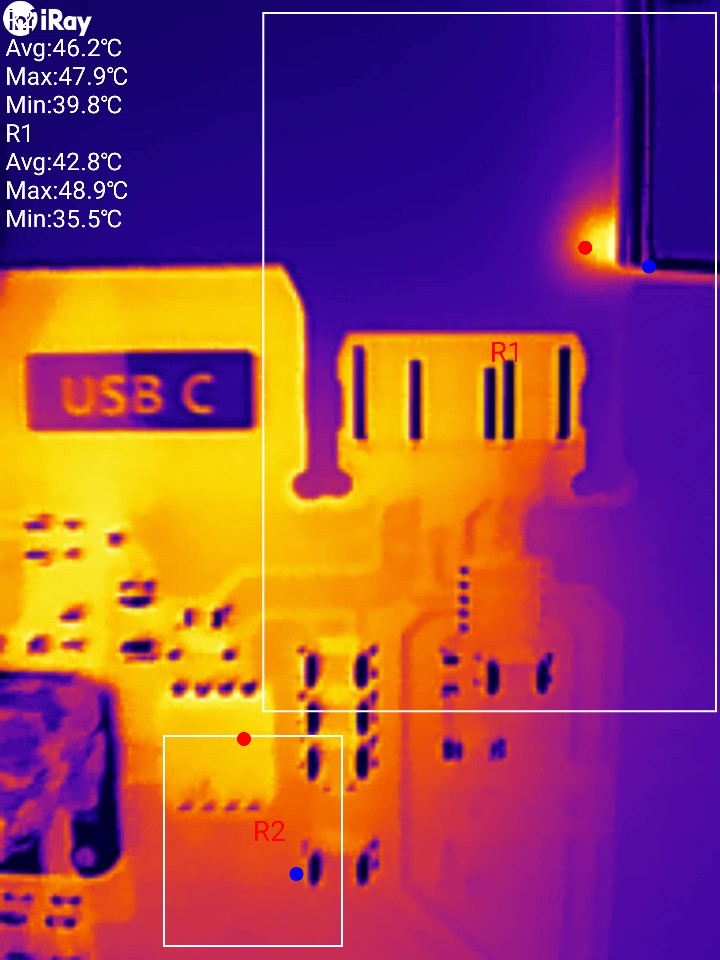
The data is now here! 100+ mating cycles later, I have included microscope photos, thermal tests, and measured how much force it takes to break this connector. All updates are on GitHub: https://github.com/AnasMalas/pcb-edge-usb-c My previous post talked about why I created these footprints (https://www.linkedin.com/posts/anasmalas_what-does-it-take-to-make-the-slimmest-possible-activity-7387799941340979200-p10Q).
I am very grateful for the large engagement on here and on X! Hackaday even wrote an article about it, and it was within the top page on Hacker news! I love that this could potentially be helpful to so many, but as many in the replies pointed out: This is a much less durable connector, and you should keep that in mind before deciding to use it! While I had tested the connector on my contact card, I did not document it at the time.
You can find the new tests and a new 24 pin fully featured KiCad footprint in the GitHub repo linked above, and please tag me when you post about the cool stuff you make with this :)