Integrated circuits (ICs) keep getting smaller and faster, so it is increasingly important to design circuit boards correctly.
Firstly, if you dont understand return currents well, I implore you to watch the presentation that changed my life, by Rick Hartley: https://lnkd.in/dECCj99s
I have talked to many designers who know return currents, but recommend counter-productive stackups. Let's start with a basic fact: A signal layer must have an adjacent, relevant, and close return plane. When you move a signal through layers, so does the return. how it does so is the question.
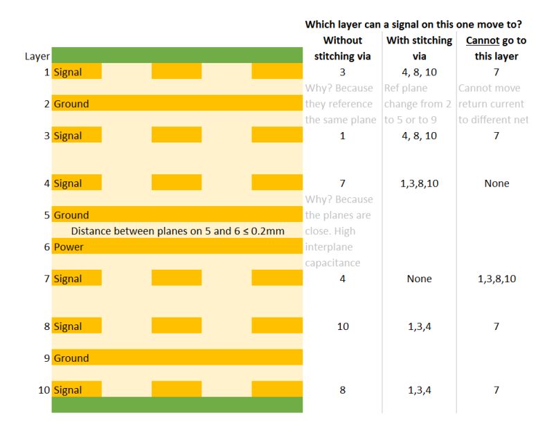
The first attached stackup photo is a 10 layer stackup taken from Susy Webb's presentation: https://lnkd.in/dP8Wph5C. It illustrates the cases you could face in any design. A signal on layer 1 has its return on layer 2, with the energy traveling in the dielectric between them. If you move the signal to layer 3, the energy will pass through the barrel's antipad and continue between layers 2 and 3. The current doesnt change layers, and the energy doesnt spread.
On the other hand, say you want to move a signal from layer 1 to 8. If you dont include a stitching via that connects the grounds on layers 2 and 9, the return current will spread wide and "force" itself through your circuit until it finds layer 9. A stitching via provides a good path and the energy wont spread.
But you'll see something interesting, how can a signal on layer 4 go to 7 at all? The distance between the two planes is small, so the return current can find enough capacitance to flow without spreading widely (remember, C∝A). However, going from layer 7 to 8 doesnt work well, as you cannot directly stitch or couple layers 6 and 9 together.
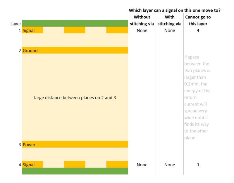
That brings us to the first 4 layer stackup. See the issue? The planes are far away so if the signal changes layers from 1 to 4, the return current will spread very far until it finds enough capacitance to couple from layer 2 to 3. Some designers recommend this with "layer change capacitors" to move the return from layer 2 to 3.
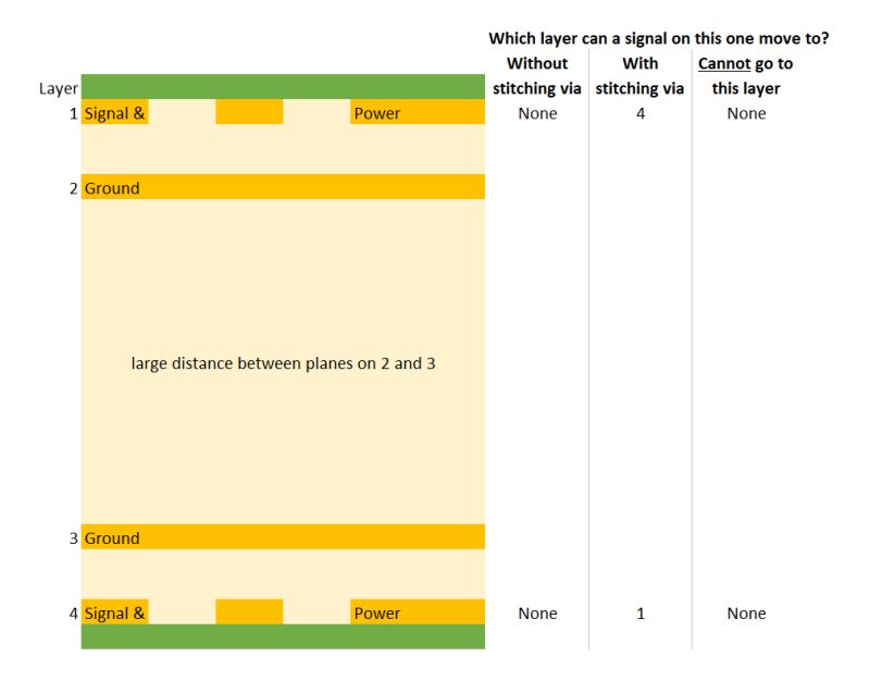
However, looking at a $0.5 mcu's (Attiny5) IBIS model reveals that its rising waveform can be as fast as 1 ns (no load). That's an edge frequency of 1 GHz, and a 0402 0.1 uF capacitor resonates below 30 MHz, not to mention via inductance. The second 4 layer stackup allows for stitching vias and provides a return to power, which is why I believe it is better for today's designs.
Here's where id appreciate some help. In an article, Lee Ritchey said that stitching vias aren't necessary. I believe he's talking about high density designs which have tons of ground vias anyway, but that's speculation. Also, in the 10L stackup even if layer 3 is twice nearer to its reference than layer 4, wouldnt there be crosstalk between them?
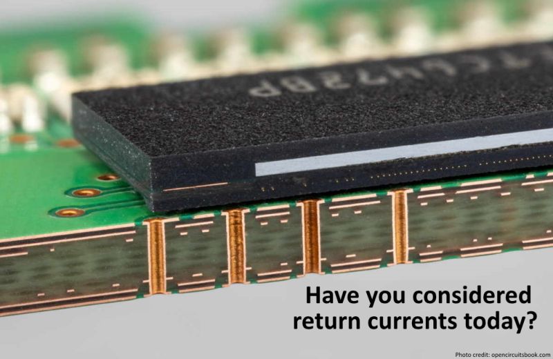
Cover photo taken from opencircuitsbook.com. Excited to get my copy!