During PCB West 2024, two talks gave me reasons to remove copper, soldermask, and silkscreen from under my 2-pin components (resistors, capacitors, etc) for different reasons I hadn't considered. Let's explore why.
Preface: Today, PCB design cannot be treated like laying wires. Almost all modern PCBs contain signals with high frequency content. For those, it is important to have a nearby uninterrupted "return" where "return current" will flow. The closer the two are together, the lower inductance will be.
But where is the energy really contained? Is it the current in your traces? Is it in the voltage?
Daniel Beeker made his intention to brainwash us clear, repeating "Its all about the space". His daughter even made a song about it https://lnkd.in/dTfCfd23
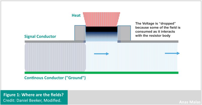
The energy in any electric circuit is contained within the EM field in the dielectric (the insulator). In your PCB that's the fiberglass-resin between your copper layers, and in a grid transmission line that is air. So if the field is between a trace on layer 1 and a ground plane on layer 2, what happens when it reaches a resistor?
As the fields of your signal propagate, they reach the resistor and use use its body as a continuation of the trace, as seen in figure 1. If there is a ground flood on layer 1 and it goes under a resistor, this impedes the field (especially for signals with high frequency content). Capacitors store and release fields which should be able to go in and out with the least impedance, which you can achieve by using the smallest possible capacitor package and exposing its body to the adjacent plane.
Worse yet, running traces under resistors causes crosstalk. This may be fine for slow analog signals, but digital signals are very fast. Adding a keepout in your footprints prevents copper under your components and solves this issue (do however add a copper island with ground vias under ICs).
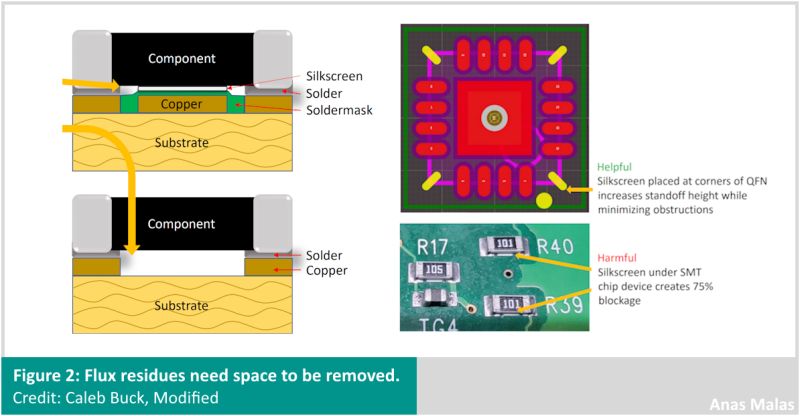
In another session, Caleb Buck shared his experience in design for reliability, with a focus on flux types and residues. Caleb did a series of tests using methods like "SIR" to test footprints for residue retention. While no-clean flux residue has the lowest (but present) chance of failure, cleaning most components with water or chemicals was sufficient to remove the residues. However, some components did retain flux after cleaning, especially resistors and capacitors. This is because the body of these components rests directly on the PCB with no gap, as seen in figure 2.
The solution is simple. By removing copper, silkscreen, and soldermask from under and a resistor's body, there is enough room for cleaning these residues. QFN packages have a similar issue, and using diagonal silkscreen lines can help lift the package slightly and channel cleaning fluid in.
Small, simple changes, towards designs that work right the first time.